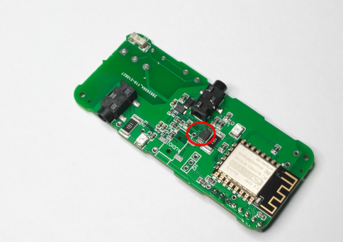
The latest PCBs for the CU monitor arrived this week. They were supposed to be the test batch to prove the release of the CU Monitors to the website. There followed a frustrating two days of soldering up and testing. Essentially I had the surface mount ADS1115 that needed to be soldered onto the board. These are tiny chips that can be tricky to solder. After soldering 3 boards I had one that worked intermittently and two that just plain failed to work. So I looked at the working one on the bus analyser and the timing of the I2C bus seemed to be causing a lot of NAKs. After tweaking the software driver, this became a lot more reliable, which suggested the bus layout on the PCB was bad! making the communication timing marginal.
This means this will not be the last board! This got me thinking. The ADS1115 is a fairly low cost 16 bit A to D converter, initially I chose this chip because it was a module that lends itself to rapid prototyping but it has 4 channels and is accessed across an I2C bus. This chip has caused me to redesign the CU Monitor PCB in the past because we are reading more than one channel rapidly it can cause significant slow down in the sample rate. Currently the CU monitor only uses one of the channels to boost the read speed. This makes this chip way over specified for our purpose.
So I intend to reassess the use of this chip and I will create a sequence of design/posts and explain my design decisions to document this procedure and help me get it straight in my mind